|
|
Instrument of the Month June 2015 |
|
|
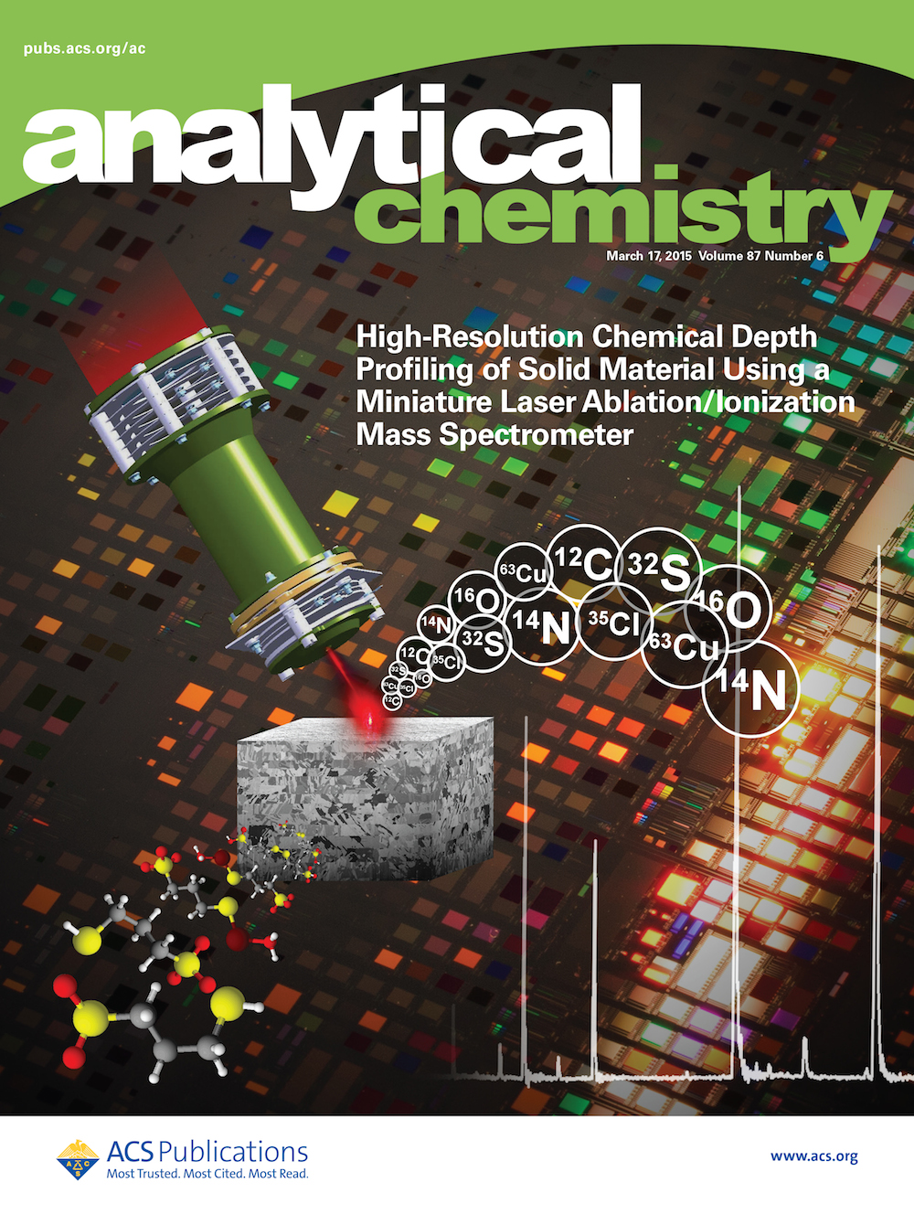
Novel Depth Profiling Technique Based on Laser Ablation Mass Spectrometry |
||
|
||
|
Laser ablation mass spectrometry was employed to quantify impurities incorporated in a copper matrix that was deposited by an additive-assisted electroplating process. This process is used in the semiconductor industry for the fabrication of interconnect architectures in logic and memory devices.
This work was carried out in the group of PD Dr. Peter Broekmann in collaboration with the group of Prof. Dr. Peter Wurz from the Space Research & Planetary Sciences division at the University of Bern. References:
|
||